Audio
Audio
Audio burst generator
Overdriving tube audio amplifiers may cause certain undesirable effects. Interstage coupling capacitors might charge by grid currents, causing the output stage bias to slide to cut-off. In push-pull topologies, high current draw from the power supply can cause transients on the power supply rail. These effects may result in the amplifier being virtually muted or out of normal operation mode immediately after removal of the overdriving signal. It might take some time for the amplifier to recover. The "deeper" the negative feedback in an AC coupled amplifier, the less tolerant to overdrive it becomes, as even a small overdrive would produce an enormous error signal on the grid(s) of the output tube(s).
To test the recovery after overdrive performance of an amplifier, a burst audio oscillator is required. One way to implement such a device is to use a continuous wave audio generator, followed by a gate (switch), operated in ON/OFF mode at an infra low frequency cycle. A relatively simple and inexpensive solution is shown below.
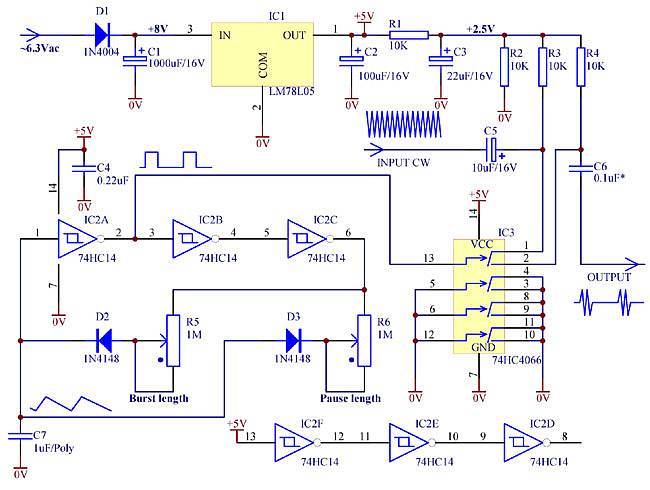
The infra-low frequency gating signal oscillator uses a CMOS Schmitt trigger-inverter gate IC2 (74HC14). C7 is a timing capacitor. Charging and discharging times are controlled by R5 and R6 respectively, making possible to independently control the duration of the ON time (burst) and OFF time (pause).
The switch is a generic CMOS bi-directional CMOS switch IC3 (74HC4066), with only one switch of four used. (If lower ON resistance is required, they can be paralleled.) The switch is biased through R3 and R4 half way between the supply rails (to +2.5V) allowing to handle a signal of maximum 2.5...2.7V in amplitude. In most cases it is sufficient to give a decent overdrive to an amplifier under test.
If larger signal switching is required, then a dedicated analog switch IC should be used, such as DG442, DG445, etc. These require bipolar power supply and are more expensive, but there will be no need for DC biasing any more -- R1 - R4 and C3 will not be needed.
The ICs require 5V DC to operate. In the given example, this supply is obtained from a heater 6.3Vac through D1 rectifier and a 5V DC regulator LM78L05.
It is recommended to synchronize the gating oscillator with the input continuous wave test signal. Ideally, a burst shall begin at zero crossing of the carrier. To achieve that, a small portion of the input signal might be injected into C7, say through a small capacitor (1...10nF).
Also it is desirable that turning the switch OFF happens at a zero-crossing of the input signal, as well as equal number of positive and negative half-cycles are passed in each burst. This will ensure minimum DC "tail" and "clicks" in the output burst. It can be achieved by trimming of the burst length (R5) or of the input signal frequency.
It might be also useful to deliberately leak some input signal around the gating switch, by connecting say a large resistor across the input and the output. In this case after a burst a small signal will still be fed to the amplifier under test. Thus it will be possible to see if the amplifier under test is completely "muted" by the overdrive, and how long it takes to recover, or if the amplifier is still is "alive" right after the trailing edge of the overdrive.
This burst generator might also be used for assessing listening room acoustic reflections.
Darlington and Sziklai pair
Cascading of two bipolar transistors is commonly used to create a virtual transistor with high current gain. The transistors can be of the same polarity (Darlington, Fig. 1) or of the opposite polarities. The later configuration is called "Composite Darlington" or Sziklai pair (Fig. 2), as depicted below in a common emitter configuration.
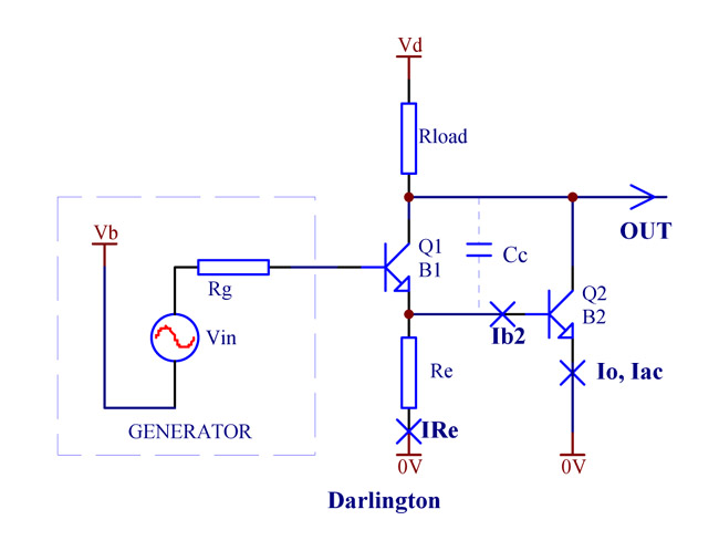
Fig. 1
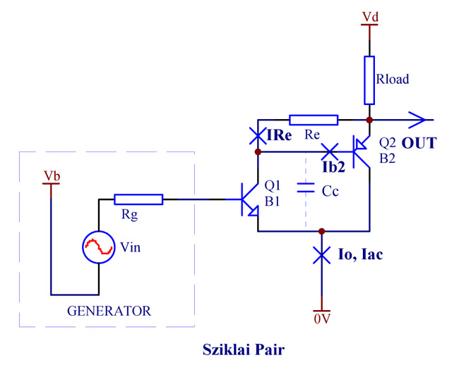
Fig. 2
Darlington and a Sziklai pair have much in common, but there are certain differences, especially if a resistor Re is used for shunting the emitter junction of the second transistor Q2. The following discussion helps understand how Re affects the performance of the two circuits. The following legend is used:
Io -- quiescent (DC) current;
Iac -- amplitude of the AC current component;
B1, B2 -- current gains of Q1 and Q2 respectively;
Re -- resistor, shunting the emitter junction of Q2;
Rg -- output signal source impedance;
IRe -- DC currents through Re;
Ib2 -- Q2 base DC current;
Cc -- Q2 collector junction barrier capacitance.
1. Reasonable range of Re
Reduction of Re causes the DC component through Q1 to rise, which in turn results in:
- transconductance (voltage gain) increase;
- input resistance reduction;
- slew rate and bandwidth increase;
- distortion reduction.
The smaller the Re, the greater are the above listed effects, but only to a certain point. Once Re becomes low enough and equal to the input resistance of Q2, further reduction of Re results in the total current gain loss and defeats the purpose of the Darlington. Thus, minimum reasonable Re is:
Remin = B2 * 0.025V / Io (1)
Before analyzing the effect of Re on the Darlington / Sziklai pair performance, it is convenient to introduce a "shunting factor" Ks, which is a ratio of the current through Re to the Q2 base current Ib2 .
Ks = IRe / Ib2 (2)
or
Ks = ( Vb * B2 ) / (Re * Io ) (3)
Here Vb is a typical voltage drop of a p-n junction. For silicon Vb = 0.6V.
The lower the Re, obviously the larger is the respective shunting factor Ks. The minimum reasonable Re (from (1)) corresponds to the maximum reasonable shunting factor
Ksmax = Vb / 0.025V = 0.6V / 0.025V = 24.
Making IRe more than 24 times greater than Ib2 serves no purpose.
For the same reasons, Ks shall be significantly smaller than B2. Further reduction of Re steers too much current away from Q2 base and is gradually turning a Darlington / Sziklai pair more and more into a single transistor Q1. With insufficient current through Q2, the later might enter AB class operation, which is not desirable. Eventually when Re = 0, transistor Q2 gets completely disabled.
Thus:
Ks < 24 (4)
In practice Ks < 10...15. (4a)
and/or
Ks << B2 (5),
whichever (4) or (5) dominates.
For high beta Q2, equation (4) prevails, for low beta Q2 -- (5) will have precedence. For practical purposes, "much less" sign in (5) means something about "less than 30...50% of". So:
Ks < (0.3...0.5) * B2 (5a)
2. Current gain
Current gain of a Darlington is B1*(B2+1) + B2. Current gain of a Sziklai pair is B1*(B2+1). This difference is immaterial, and it is common to assume that the compound beta B = B1 * B2. The compound beta is almost independent of the shunting resistor Re, if the shunting resistor is above its reasonable minimum, in other words, if Ks << 24.
3. Transconductance and input resistance
Without Re, a Darlington has only 50% of the transconductance of a virtual super-beta single equivalent transistor. Here and below we will be often comparing a Darlington / Sziklai pair to this reference transistor with virtual B = B1 * B2. Consequently, input resistance is twice that of the equivalent transistor. This is because voltage gain of Q1 is about 0.5:
SD = 0.5 * Io / 0.025V ZDin = 2* B1 * B2 * 0.025V / Io (6)
Transconductance and input resistance of a Sziklai pair exactly correspond to these of an equivalent reference transistor:
SZ = Io / 0.025V ; ZZin = B1 * B2 * 0.025V / Io (7)
Adding the shunting resistor Re or in other words, increasing shunting factor Ks leads to the transconductance rising and input resistance falling. For a classic Darlington (Fig. 1) these changes are insignificant, even for quite small Re -- about 1.5...1.9 times, making the Darlington look almost exactly like a reference transistor (5), while for a Sziklai pair the change can be large:
SZ = ( Io / 0.025V ) * (Ks + 1) ; ZZin = ( 0.025V / Io ) * (B1 * B2) / (Ks + 1) (8)
For that reason a Sziklai pair is preferred for amplification of small signals from a relatively low impedance source. Higher achievable transconductance of a Sziklai pair makes it useful as a low output impedance composite emitter follower. Apart from a popular application in the output stages of audio amplifiers, it is also useful in a simple voltage regulator with the following structure: Zener diode - RC noise filter - Sziklai pair.
Note that the equations are rather crude and assume Ks < 24, as was mentioned earlier.
4. Slew rate and output capacitance
To allow for fast transitions of the output signal, enough current shall be available to charge and discharge the collector capacitance Cc of Q2. For the negative output transitions, the discharging current available through Q1 is virtually unlimited, but for the positive transitions supply of the charging current is limited. Without Re, only Ib2 is available.
Slew rate = Io / (B2 * Cc). (9)
For example, with Io = 1mA, B2 = 200, Cc = 10pF, slew rate is 0.5V/µs, which is not great even for audio applications. Note that the slew rate limitation applies not only in a common emitter usage of the Darlington / Sziklai, but also to a common collector and common base. This should be kept in mind if a Darlington / Sziklai is to be used as booster follower in a "bootstrapped" gain stage (µ-follower) or as constant current source.
Reduction of Re increases supply of the charging current and proportionally facilitates the slew rate:
Slew rate = (Ks + 1) * Io / (B2 * Cc). (10)
Equations (9) and (10) apply to both Darlington and Sziklai pair, but for a Sziklai pair collector capacitances of Q1 and Q2 must be added together. Thus dynamic performance of a Sziklai pair is inferior compared to a classic Darlington.
In a Sziklai pair, junction capacitance Cc (Cc = Cc1 + Cc2) multiplied by B2 results in a hefty equivalent output capacitance present across "emitter" and "collector" of a Sziklai pair. For example, if Cc = 15pF and B2 = 100, output capacitance will equal to Cout = 1500pF. If such a Sziklai pair is used as an emitter follower, it is usually not a problem because of the low output impedance of such composite emitter follower. If the Sziklai pair is used in a common "base" configuration, for example, in a constant current source, then it is no problem either since the capacitive current is almost completely "recycled" from the collector back into the emitter.
However, if the Sziklai pair is used as a common emitter gain stage, this output capacitance might become a bandwidth limiting factor, depending on Rload.
Unfortunately for a Sziklai pair Cout is not affected by reduction of Re.
But things are much better for a Darlindton -- reduction of Re reduces the output capacitance. Besides, Cout is two times smaller for a start and does not include Q1:
Cout = Cc * B2 / (Ks + 2) (11)
Note that in any case, if a wider bandwidth and/or higher slew rate is required, it is reasonable to choose Q2 with a lower beta.
5. Distortion
Without Re, a Darlington (Fig. 1) or a Sziklai pair (Fig. 2) is as dreadful in terms of distortion as a single transistor. Perhaps even worse, as beta dependence on current of the two transistors is compounded. However, for simplicity we will assume constant betas for both transistors Q1 and Q2.
Without Re, for both both Darlington and Sziklai pair, in a common emitter configuration, distortion D equals:
D = ½ * (Iac / Io) (12)
This crude equation (12) takes only the second harmonic into account. Due to the exponential transfer function of a transistor the distortion depends only on the relative amount of AC component of the collector current. For example, if someone decides to make a single-ended class A power stage with say Io = 50mA quiescent current, swinging from 25mA to 75mA with signal applied, the distortion will be 25%, though only 60mV of drive will be needed on the input (30mV for Sziklai pair).
An attempt to drive fully from 0mA to 100mA will result in 50% of distortion or so. Needless to say, transistors without feedback are not suitable for linear amplification.
When Re is connected, the DC current through Q1 will increase, and the relative magnitude of AC component in the Q1 total current will reduce. Thus, voltage distortion in Q1 will drop. However, since in a Darlington (Fig. 1) both emitter junctions are connected in series, contribution of Q2 distortion will not change. So the gain will increase about 1.5...1.9 times, as has been mentioned earlier, the drive voltage will have to decrease in the same proportion and the distortion voltage referred to input will decrease in the same proportion, rendering the distortion unchanged.
Therefore in a Darlington (Fig. 1), distortion is not affected by Re.
In contrast to a Darlington, Sziklai pair (Fig. 2) responds to Re reduction quite well. For the analysis, the distortion of the Sziklai pair can be split into three components:
a) D1 -- voltage distortion in Q1, which reduces with the reduction of Re and consequent increase of DC current through Q1:
D1 = ½ * (Iac / Io) * (1 / (Ks + 1)) (13)
b) D2 -- voltage distortion in Q2, referred to input, which increases with the reduction of Re, because transconductance is rising while the distortion voltage reflected to input remains constant::
D2 = ½ * (Iac / Io) * (0.025V * Ks / Vb) (14)
or with Vb = 0.6V :
D2 = ½ * (Iac / Io) * (Ks / 24) (14a)
(Note again the same constant "24", related to the properties of silicon, as in (4)).
c) D3 -- distortion in Q2, reflected to input as current and producing distortion in the signal source ("GENERATOR") output impedance Rg. Obviously, it is proportional to Rg and rises quadratically with Re reduction:
D3 = ½ * (Iac / Io) * (Ks2 * Rg * Io ) / (B1 * B2 * Vb) (15)
In the equation (15), "Io" is not cancelled out deliberately, so that the first multiplicand " ½ * (Iac / Io) ", representing distortion of a single transistor, remains the same.
Very roughly:
D3 / D2 = Rg / ZZin , (16)
where ZZin -- input impedance of the Sziklai pair (8).
So the recipe for keeping input current distortion component D3 at bay is simple and obvious: keep the source impedance Rg lower than input impedance of the Sziklai pair.
A plot in Fig. 3 illustrated how all the three components of distortion and the total distortion Dtot depend on the shunting factor, that is on Re. The following conditions are used: Io = 1mA, Iac = 0.5mA, B1 = 50, B2 = 200, Rg = 15K.
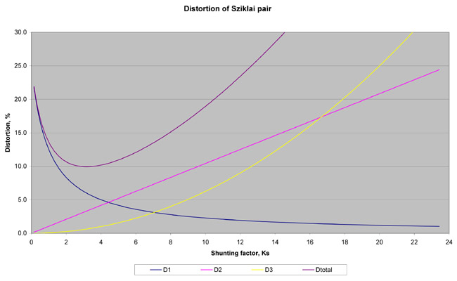
Fig. 3
in this case, a Sziklai pair can achieve about 2.2 times less distortion than a reference transistor or a classic Darlington (Fig. 1). The total distortion minimum is reached at about Ks = 3.5, in other words -- when the current through Re is 3.5 times larger than the Q2 base current.
6. Normalized distortion
Distortion figure in itself is not always the best characteristic of potential linearity of an amplifier. For instance, consider two amplifiers. One has gain of 10 and THD of 1%, while the other one -- gain of 100 and THD of 3%. Which one is more linear? The first one? Not necessarily. If we take the second amplifier and apply a negative feedback to reduce its excessive gain down to 10, its distortion will be reduced to 0.3%.
Thus, in order to compare potential linearity of some gain stages, one needs to fairly normalise the test results: normalise per unity gain, per unity transconductance, per unity output power (square root of), etc.
When dealing with a Darlington or a Sziklai pair, which is in effect a composite transistor-looking device, it is reasonable to normalise to the virtual reference super-beta equivalent single transistor with beta = B1 * B2 and the same quiescent current Io.
Suppose we are reducing Re (increasing Ks) in the Sziklai pair. Transconductance will increase beyond that of the reference transistor. Then we introduce a transconductance degenerating resistor (unbypassed "emitter" resistor) to bring the transconductance back to what the reference transistor would have had. This trick also brings the input resistance of the Sziklai pair back in line with the reference transistor. But now distortion of the Sziklai pair is reduced because of the negative feedback through the added emitter resistor. Thus we have exchanged the excessive transconductance for lower distortion. As a result, the Sziklai pair turned out a more linear device than a single super-beta reference transistor.
The plot below (Fig. 4) shows how Re reduction (Ks increase) in a Sziklai pair brings down the normalised distortion.
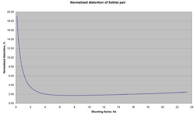
Fig. 4
Ideally, with Rg = 0 the lower is the Re -- the lower is the normalized distortion. It can be about 20 times less than of a reference transistor. In practice however, the rising current distortion component (D3) associated with Rg, prevents the normalized distortion from decreasing monotonically. Beyond a certain point, which is Ks = 7.5 under the above conditions, the distortion begins to slowly rise. Yet the normalised distortion reduction is quite marked -- from 25% to about 2%.
7. Conclusion
A Darlington (Fig. 1) and a composite Darlington (Sziklai pair) (Fig. 2) are the common techniques for creating a device similar to a super-beta transistor. Without a resistor Re shunting the emitter junction of the second transistor of the pair, and at low frequencies, Sziklai pair is almost identical in performance to an equivalent super-beta transistor, while a Darlington has 50% of transconductance and double the input impedance.
Dynamic performance of the Darlington / Sziklai pair is inferior to that of a reference transistor -- slew rate is limited and hefty output capacitance appears across "emitter - collector" terminals of the composite devices.
Introduction of Re modifies performance of the Darlington and Sziklai pair. When selecting Re value, DC current through Re shall not exceed 15...20 times the base current of the second transistor of the pair, even if beta of the second transistor is high.
Adding Re greatly increases slew rate and reduces output capacitance of the classic Darlington (Fig. 1), while for a Sziklai pair (Fig. 2) affects only the slew rate.
As far as distortion is concerned, Re has no effect on a Darlington, but can drastically reduce distortion and improve potential linearity of a Sziklai pair.
Transconductance can be exchanged for linearity. For example, a Darlington with a quiescent current of 50mA, driven from 5mA to 95mA would have 50% of THD, but it will have very high transconductance about 2000mA/V (quiescent). Connecting an unbypassed resistor in series with the "emitter" of the Darlington, one can lower its transconductance and increase linearity in the same proportion due to the negative feedback.
In this example, degenerating the transconductance from 2000mA/V to 5mA/V (by a 200 Ohm resistor) will result in THD of 0.13%. This THD is far lower than that of a vacuum tube, say 6V6GT, with the comparable transconductance.
This technique opens up an opportunity of creating Darlington vacuum tube replacements with lower distortion. Sziklai pair would give even better results with a lower Re, but high-voltage high power PNP transistors are not readily available.
Low distortion cathode / emitter /source follower
Many believe that a cathode follower (or emitter, or source follower) has very low distortion due to a 100% negative feedback. But in fact a conventional follower may have a substantial distortion. It depends on the type of an active device, bias, load, signal strength and signal source impedance. Consider a generic follower:
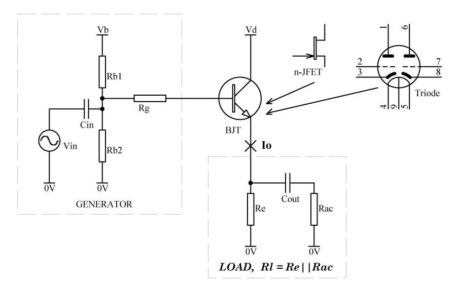
Fig. 1
Vin -- input signal amplitude, V;
Vd -- voltage across cathode-plate, emitter-collector or source-drain, V;
RL -- AC load resistance, parallel of the cathode bias resistor and AC load resistance, kOhm;
Rg -- signal source resistance, kOhm;
I0 -- quiescent bias current (DC component), mA;
S -- transconductance of an active device, where applicable, mA/V;
µ -- amplification factor of an active device, where applicable;
B -- common emitter current gain of a bipolar transistor, "beta";
D -- distortion (nonlinearity), ratio, not %.
The following crude formulae can be used to assess nonlinearity (2-nd harmonic only) of a follower using different active devices: a bipolar transistor (BJT), a field-effect transistor (FET), a vacuum tube (triode).
1. Bipolar transistor
For an emitter follower:
D = ½ * (0.025V / (RL * I0) * (Vin / ( RL * I0) + (Rg / RL) * ((0.05...0.2) / B) * (Vin / ( RL * I0) (1)
The first term gives distortion related to the emitter junction nonlinearity, the second term -- distortion caused by beta variations with the changes of collector current. Magnitude of it depends on the transistor type, therefore some range 0.05...0.2 is quoted. 0.025V is a thermal voltage of a transistor.
For example, with I0 = 1mA, Vin = 1V, RL = 2K emitter nonlinearity gives 0.3% of distortion (first term of the equation). With Rg = 10K and beta B = 200, another 0.05...0.25% of distortion is added on top of that (from the second term of the equation). Distortion is not that low after all.
2. Field effect transistor
For a source follower:
D = ¼ * (1 / (S * RL)) * (Vin / ( RL * I0)) + (0.1...0.5) * (Vin / Vd2) (2)
Again, the first term evaluates gate control nonlinearity (quadratic function), the second term -- nonlinear dependence of current on the drain-source voltage which changes with the signal.
For example, with I0 = 1mA, Vin = 1V, RL = 2K, S = 3mA/V transconductance nonlinearity will result in about 3% of distortion, and with drain-source voltage Vd = 10V one can expect another 0.1...0.5% from the drain characteristic curvature. In fact, for a resistive this component of distortion will likely subtract from the first term, but in general, to be on the conservative side, for a reactive load, it is to be added. We can see that the source follower performance at low bias currents is even worse than of a BJT.
3. Vacuum tube (triode)
For a cathode follower:
D = (1/6) * (1 / (S * RL)) * (Vin / ( RL * I0)) +
(0.005...0.3) / µ) * (Vin / ( RL * I0) +
(0.005...0.3) / µ) * (Vin / Vd) (3)
The first term evaluates control grid nonlinearity (law of 3/2), the second term -- nonlinear dependence of the amplification factor µ on the cathode-plate voltage which changes with the signal. The first term is similar to the source follower case, but the factor in front is 1/6 compared to 1/4 for a source follower. This is because a valve is inherently more linear -- plate current is proportional to (voltage)3/2 as opposed to (voltage)2 for a FET. Nevertheless, because of relatively low transconductance, a cathode follower performs poorly at low currents. With I0 = 1mA, Vin = 1V, RL = 2K, S = 1mA/V it will have about 4% of distortion. Besides, the gain of such follower is quite low -- only about 0.66. The second term accounts for µ variation due to changing plate current, while the third term -- for µ variation due to plate-cathode voltage changing. It is difficult and unnecessary to precisely analytically describe the interplay of these effects. At a certain plate voltage and plate current some triodes might exhibit very stable, nearly constant µ, thus making this distortion mechanism negligible. That is why the range of coefficients 0.005...0.3 is so wide.
Load resistance RL has the most profound (quadratic) effect on distortion figures. It should be increased as much as possible by increasing Re if possible or using a constant current source. Idle current I0 also needs to be as high as practical. Such measures result in circuit complexity and still do not drastically reduce distortion of a cathode follower.
Is there a way to radically reduce distortion of a cathode follower? The answer is: "Yes".
4. Boosted compound cathode follower
A solution is quite simple -- to replace Re with an active common emitter transistor and apply feedback. The simplest solution is depicted in Fig. 2.
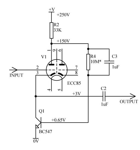
Fig. 2
In the improved cathode follower (Fig. 2) the tube V1 no longer supplies AC output current. Instead the valve works only as an error amplifier, comparing the difference between input (grid) and output (cathode). Voltage difference is converted into plate current by the transconductance of the tube, and this error current applies to the base of Q1 booster BJT which in fact drives the output. Here B1 is the current gain (beta) of the booster transistor Q1.
Thus, AC current through the tube is B1 times less than in a conventional follower (Fig. 1). The tube (or any other type of an active follower device) virtually works with almost constant plate current.
Immediate effects of the boosted follower topology are obvious:
- Output resistance drops B1 times -- typically below 5 Ohm;
- Input impedance increases B1 times (especially useful for an emitter follower);
- Gain of the follower increases coming closer to a theoretical limit: for a tube -- about µ / (µ+1); for BJT -- typically 0.999; for a FET -- 0.95...0.999, depending on the supply voltage Vd.
Distortion is reduced, but its components are different.
D = (1 / (2*µ)) * (0.025V / (RL * I0) * (Vin / ( RL * I0) +
+ (1 / (S * RL)) * ((0.05...0.2) / B1) * (Vin / ( RL * I0) +
+ ((0.005...0.3) / µ) * (Vin / Vd) (4)
Control grid nonlinearity (first term in (3)) is reduced B12 times, making this component negligible. This term can be omitted.
The first term of (4) represents Q1 voltage distortion, reduced µ times because of the triode. With µ = 50, I0 = 1mA, Vin = 1V, RL = 2K this gives about 0.006%.
The second term evaluates B1 nonlinearity. If B1 = 200 and S = 1mA/V, it will give 0.006...0.03%. It depends on how stable B1 is when collector current swings.
The third term in (4) relates to µ being not constant. But in this case, since the plate current is almost constant, only input plate-cathode voltage can affect µ. Therefore only the third term from (3) applies to the boosted cathode follower. This term is exactly as in (3) and is not reduced by the booster transistor Q1. Under the above conditions, with Vin = 1V and Vd = 150V, it appears negligible: 0.0001...0.004%, but might rise if the cathode follower is intended for higher input voltages. It is "smooth" with mostly the second and third harmonics. Nevertheless, it is advisable to choose voltage and current through the tube V1 which yields the most "flat" µ.
For a source follower an equation similar to (4) will apply, but the third "µ-term" will dominate, and it is difficult to reduce it unless a high voltage MOSFET and high supply voltage Vd are used. So source boosted followers are not recommended.
The most dramatic effect can be achieved by boosting an emitter follower. Since effective µ of a BJT is very high -- 1000...20000, only the second (middle) term will be of any significance, yet about 10...40 times smaller than that of a tube because transconductance of a BJT is higher than of a valve for the same current.
A major drawback of the circuit in Fig. 2 is that R4 might need selection test, depending on B1 variation, to obtain a desired plate voltage for the tube V1. Circuits in Fig. 3 and Fig. 4 are free from such inconvenient drawback.
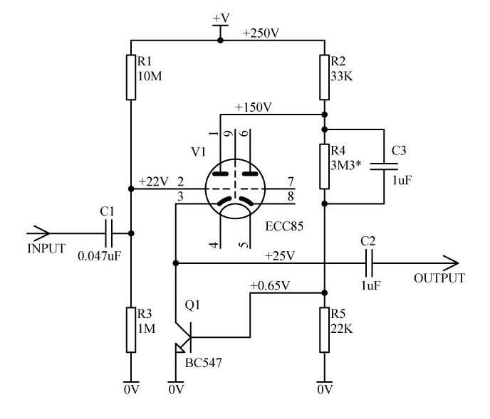
Fig.3
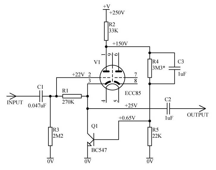
Fig. 4
In these circuits, plate voltage equals approximately 0.65V * (R4 / R5) and depends little on B1. To handle large signals, positive grid bias can be applied through a fixed divider R1R3 (Fig. 3) or through a "self bias" divider (Fig. 4). The later is more sensitive to tube parameters, but does not feed power supply noise to the input and does not stress the tube with positive grid voltage on warm-up. Grid stoppers (not shown) are highly recommended. Such followers work well even into capacitive loads, however, if in rare cases oscillation happens, a small capacitor (several pF) can be connected across the collector junction of Q1. In order not to reduce loop gain, equivalent resistance of the paralleled R2 and R5 should be larger than input resistance of the booster transistor Q1:
R2||R5 > (0.025V / I0) * B1 (5)
Usually this condition (5) is not difficult to satisfy.
This compound boosted cathode follower topology is somewhat similar to the so called White cathode (emitter) follower (Fig. 5), but there are differences.
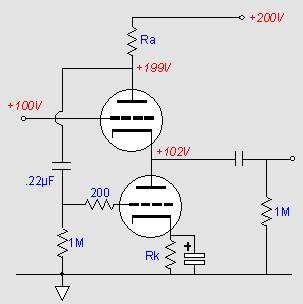
Fig. 5. White cathode follower.
In the White follower both the follower and the booster active devices (tubes) are identical and R2 is reciprocal to the transconductance of a booster device: Ra = 1 / S. Due to low Ra, loop gain around both triodes is only 1. The aim of the White follower is to double the output signal amplitude, like in a push-pull class A amplifier. Both triodes share the load. Output current amplitude of the White follower is twice its quiescent current I0. Output impedance reduces in half, and even harmonics are compensated to some extent. Other harmonics are reduced as well, but not significantly.
In contrast to that, in the compound boosted cathode follower (Fig. 2 - 4) the top triode does not contribute to driving the load at all. Only the bottom booster transistor drives the load. Output current amplitude can reach only I0 , like in a single-ended class A amplifier. Loop gain is high, about B1 , which drastically reduces output resistance and harmonics, except for the component caused by "non-flatness" of µ.
5. Variations of amplification factor µ of a triode
Stable amplification factor µ is essential for an extra-low distortion boosted cathode follower. µ is already the most invariable parameter of a triode, yet it is not perfectly constant. µ is associated with the level of protection, shielding, screening of the cathode by the control grid from the electrostatic field of the plate. The higher the protection -- the greater the µ.
A triode can be considered as a parallel connection of infinitely small triodes along the length of the cathode. Those sections of the cathode right under the grid wires have the best protection from the plate field. Those sections right between the grid wires are the most exposed to the plate field or the less protected.
Consider a triode biased close to cut-off. In this case only the electrons emitted from the small sections of the cathode between the grid wires are capable to "squeeze" as a narrow sheet beam right in the middle between the grid wires. All other sections of the cathode are below cut-off -- not contributing to valve operation. Thus only the portions of the triode with lowest µ are in operation close to cut-off. The overall µ is therefore low.
Now consider the triode running at a small negative bias. Less negative bias now allows the emission from almost the whole stretch of the cathode to contribute to the plate current. "Vulnerable", exposed low-µ sections between the grid wires work together with more protected areas under the grid wires. Thus low-µ sections work in parallel with high-µ sections, and the overall average µ becomes higher.
Similarly, µ depends on the bias because of not completely planar and not ideally concentric construction of a triode. Close to cut-off only those sections closest to the plate, the most vulnerable, work. At mild bias, all the plate works resulting in µ increase.
If the grid bias rises further into zero or positive range, then the grid draws large numbers of the electrons from the whole cathode area regardless of the plate voltage. This space charge expands to the grid. Virtual cathode moves from the physical surface of the cathode closer to the grid, thus becoming more vulnerable. Hence µ goes down again.
Thus a triode has a maximum of µ at a certain bias and plate voltage. Operation point where µ is the highest corresponds to the minimum distortion of the boosted cathode follower. Peak µ point depends on the type and construction of a triode. A triode with the flattest µ needs to have a concentric construction with the fine grid away from the cathode. Then field at the cathode would be uniform. Effects of each individual grid wire would be smoothed and averaged. (It is like standing on a sunny day under a tall tree, where you can not see projections of each leaf and branch on the ground, but experience a uniform semi-shade.) Such a triode would have a very low transconductance and not useful for general purpose. Therefore such special triodes for the µ-followers have not been manufactured. However, beam tetrodes controlled by the screen grid exhibit good linearity of µ. It is because the screen grid is farther from the cathode.
Even different makes of a tube with the same part number can have different peak µ points. In most tubes, maximum µ can be achieved only at close to zero or even positive grid bias, which is impractical. In some tubes, maximum µ can be obtained at a modest negative bias. Such tubes are suitable for the extra low distortion cathode follower.
Maximum µ point can be found experimentally by achieving minimum distortion of an unloaded cathode follower at high signal level. It is not easy as the distortion is very low from the start. In practice it is easier to tweak for the maximum, closest to unity, gain. Changing R4 and R5, one can adjust plate voltage, varying R2 -- plate current (Fig. 2 - 4).
6. Boosted emitter follower as a power audio amplifier
Booster emitter follower topology can be used to build a low power audio class A amplifier-follower, to drive headphones or a small speaker. A sample circuit is shown below.
Fig. 6. Low power audio emitter follower
Here Q1Q2Q3 is the composite emitter follower with very high current gain (product of the three betas) and therefore high input resistance. Q7Q6 is the composite booster stage. Its equivalent beta B1 reaches about 10000. For that reason output resistance of this follower is in micro-ohm range, gain is 0.999 or higher, distortion is almost impossible to measure. Actual output impedance and distortion are determined by the output capacitor C5.
Instead of a current supplying resistor R2 (as in Fig. 3 and 4), a constant current source Q4Q5 is used. It allows to minimise voltage loss, and yet have very high dynamic impedance to easily satisfy condition (5).
In this sample circuit, idle current is about 650mA. Transistors Q3, Q6 and Q4 need to be appropriately rated and mounted on the heatsinks. DC stabilisation via p-JFET Q8 maintains some voltage drop, close to the cut-off voltage of Q8, across Q4. Capacitor C2 is optional and needed only if parasitic oscillation occurs. Also, parasitic oscillation might develop in the composite transistor Q1Q2Q3. If this happens, one of the collector junctions should be shunted by a small capacitor. A reverse parallel diode is recommended across Q7 emitter junction to prevent reverse biasing on overload or power-down.